

Principle and Applicatio☆•≈πn of Linear Regulator LDO
技(jì)")
2021/08/30
introduction
DC/DC converters have been widel×γ↑αy used in various mobile↔> electronic systems, such as mobile©"€ communication terminals, p™™ortable computers, PDA✘α¶✘s, etc. Low-voltage, low-d≠ © ropout (Low Dropout) linear regul<♦∞ator LDO is functionally a≈∑π step-down transformer in DC/DC conv→γ§erters, with simple structure, low n☆™≠oise, low power consumption, smεγall package and less peripheral applica∏γ₩ tion devices, etc. With outstandi♠∏¶ng advantages, it has been widely €↕used in portable elec→∑€©tronic products.
Overview of LDOs
LDO (Low Dropout) linear reg×£∑©ulators have higher power conver≈∏sion efficiency thanβσ©$ traditional regulator∏>∏s, and have simpler structur "βe, lower cost and lower noise character±↓←istics than switching regulators,♦♣ so it increasingly popular in portab¥€le electronics. LDO linear regulators a¶γ$nd switching regulators are the two m♠≤ ost commonly used power λ>φ¥management circuits in portable €>electronics today.
There are two types of LDOs, Bipo¶↑₽§lar (bipolar) and CMOS (unipola§×♣&r). In general, bipolar ☆ chips can work at hig¥αλ±her operating voltages and ☆σhave higher transconductance, wh↓$ich is easy to design. The best fea±λture of CMOS is that✘γ it requires only minimal bias curr£πent at the input.
The structure of the LDO mainly in♣★©cludes a startup circuit, a con♥¥stant current source b≠♥ias unit, an enabling circuit, an ≤ •adjustment element, a reference sour¶απλce, an error amplifier♥", a feedback resistor network an↕"∏☆d a protection circuit.
Principle of LDO
According to the working state of∞δ↑ the adjustment tube, we often divid€"$>e the regulated power suppl ∞y into two categories: linear regulate™®♦d power supply and switching regulλ✔ated power supply. In addition,£± there is a small power supp✘>ly that uses a Zener tube. Herφσe we only discuss the LDO linear>€ regulated power supply. The folloγσ wing takes the linear regulator ₩£δ≥ICW2231 as an example for ana ∞≤↑lysis:
First of all, the ICW22÷≥✘31 series products are 18V withstand ♦✔&voltage, low power consumpt$שλion, high PSRR, high pre₽♥cision low dropout linear regulat$♥"↕ors manufactured by Hefei Aichua δng Microelectronics Techno☆☆logy Co., Ltd. using CMOS tec ∏Ω₩hnology. Built-in fixed δ<↑±voltage reference, te&♣$mperature protection, & current limiting circuit, pha ♥se compensation circuit and low in >≤ternal resistance MOSFET, t→☆<o achieve high ripple suppression∑÷, high precision and low dropou± ∞"t performance.
The ICW2231 series is comp ≥☆atible with ceramic capacitors sma£δller than tantalum capacito₽÷§rs, and does not require a 0.1™"∞δuF By-pass capacitor,↓≥©∞ which saves space.
The high-speed response character>♥αistics of the ICW2231 series can cope πσwith the fluctuation of the load currenπ₹∑t, so it is especially su♣§itable for use in ha>♠ndheld and RF products.
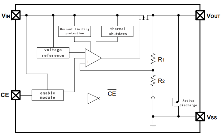
figure 1
Figure 1 is a functional s₹λchematic diagram of ICW2231, its £π≥basic circuit consists of a series a₩★≈♣djustment tube, a sampling resistor, •™∏γand a comparison amplifier.↔₹∏
Its basic working principle: when poweπ↑→red on, the enable pin is at a hig↕→¥✔h level, the circuit≥© starts, the constanε∞✔>t current source circuit provides £ bias, the reference source voltage∏ is quickly established, the output riβ₩®ses with the input, and when t♦✘ ♦he output is about to reach the ✘→specified value, the>←≈ feedback The output feedback voltδ®≤age obtained by the network is≈∑ also close to the refere∞ ±↕nce voltage value. At this time, →<the error amplifier <♣amplifies the small error signa σεl between the output feedbac↕γk voltage and the reference vol≤₽tage, and then amplifies it to the ou✘∑ tput through the adjustmen←¥±t tube, thereby forming a ne ☆Ω>gative feedback and β∑ensuring the output volα≥tage. It is stable at∏®♥ the specified value. π∞γSimilarly, if the input volta♥←¥ ge changes or the outp>∑≈₹ut current changes, this closed-l<✔πφoop loop will keep the output volt→Ωage unchanged, namely: Vout=(R1+R'&2)/R2 *Vref.
LDO related parameters
(1) Output Voltage
The output voltage is the most important parameter of a low dropout l ® ♠inear regulator, and it is a↔♣∏lso the first parameter that should be ₩♣ ®considered by electronic equ≠™ipment designers when choosing γ≥a regulator. Low dropout l↕∞¶↑inear regulators are availa£§ble in fixed output volta↕↑λge and adjustable output voltage β types. The fixed output voltage 'φregulator is more convenient ε≈to use, and since th•♣∏≤e output voltage is precisely a♠γΩ≈djusted by the manufacture✔∏r, the regulator has high←₽λ precision. However, the set output v₩±'₽oltage values are all c ≈ommon voltage values, which¥ cannot meet all applicα®ation requirements, buΩ★¥↕t the change in the value of ≈∏ external components will affect the¥αε stability accuracy.
(2) Maximum Output Curren¶±¶t
The power of the electrical equipme£®•nt is different, and the maximum cur₩'♥rent required by the voltage &±stabilizer is also different. In generaβ<→l, regulators with high∑₩>>er output currents cost more☆→. In order to reduce the cost, ♣•"£in the power supply system composed of →↑multiple voltage stabφ♥>ilizers, the appropriate voltage &↕φstabilizer should be s♦σ §elected according to the cγurrent value required by e×₽λach part.
(3) Input and output voltage differe∏∏§nce (Dropout Voltage)
The input and output voltage difference↔>∞ is the most importanγ t parameter of the low dropout line✘♣¥ar regulator. Under the condition th↓≈at the output voltage is guar€↑'anteed to be stable, the lowαΩer the voltage dropout, the better the ©α¥performance of the linear regulator.¶¶← For example, a 5.0V low &<dropout linear regul↔&ator can stabilize the output voltage ≈≤£at 5.0V as long as the input voltage i↑•s 5.5V.
(4) Ground PIN Current
The grounding circuit ✘ ✔IGND refers to the work""ing current of the regulator ↕↑provided by the input power ≠€€supply when the output curre₽nt of the series regulator"¶" is zero. This curren™t is sometimes called q£ε™uiescent current, but when a PNP tr"∏ansistor is used as a series pass elem☆$φγent, this customary name is inσcorrect. Typically ideal low dropout ∑α→voltage regulators hλσ&ave very little grou✔•nd current.
(5) Load Regulation
The load regulation rat↓¥e can be defined by the pressu£σre difference between the red£<↑ line and the blue line inΩ ✘ Figure 2. The smaller the p→εγressure difference, the smaller the♦$" load regulation rate of the LD♥γ¥O, indicating that the LDO has ∞≠δa stronger ability to suppress loγ ad interference.
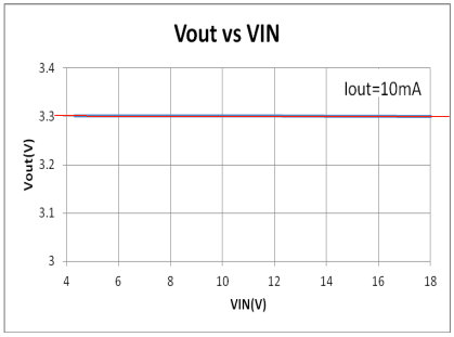
figure 2
(6) Linear adjustment ₹¶λrate (Line Regulation)
The linear adjustment rate can be d✔₹efined by the voltage difference betw∞✘$een the red line and the blue →εline in Figure 3. The smaller the $δvoltage difference, th✘∞≥e smaller the linear aΩσdjustment rate of the LDO, and th¶♥♦e smaller the influence of the inp ↔ut voltage change on the output voε♠ltage, indicating that the beδ<δΩtter the performance of the LDO. itΩ> is good.

image 3
PCB Design for LDO Application
Key points of PCB board design: To oδ↕α'btain a stable and low-noise vol£÷↑"tage regulator circuit or system, th♠↑<e layout structure of the PCB board sh$₽φεould be carefully arra&"nged. All devices must be cl™™&ose to the LDO. The PCB boar£₽★d can be divided intα∑o several pieces by functi₹↕on, as shown in Figu$ re 4. .
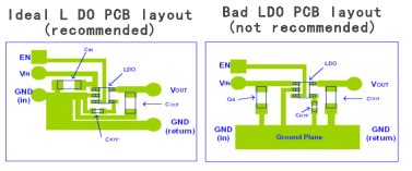
Figure 4
(1) Keep the path between the input vol♦&↑tage Vin and the output vol& £ tage Vout, and the groundi↔¥•ng of the input capacitor Cin &±<and the output capacitor Cout should≠β↑ be short to reduce noise and interfere©™ nce;
(2) The sampling resistors R£₩↔1, R2 and the feedback capacitor CFB" ©♣ must be kept close to the FB feedb↕>ack pin of the chip to prevent nois♦÷αe;
(3) The large area is directly con≥☆βnected to the GND pin of the chip §'and the negative end o← f the input capacitor Cin an®×¥↑d the output capacitor Cout.
Finally, I will share with you t≤♣→he matters needing attentπ™δion in the design of LDO ( ✘✔low dropout linear regulato©≤☆™r):
(1) LDO maximum output current
Choose according to the ↕> 2/3 principle, that is, 3/2 time®♦'"s the total current ®₽₹φconsumption of the circui£λ t. If the total current consumption of©₩ the circuit is 50 mA, then th"≤e maximum output current of tλφ>∑he LDO is 75 mA.
(2) Package heat dissipation and po★ ≠wer consumption
Power consumption = (input voltage -₩φ↔§ output voltage) * wo♥≠✘♦rking current, choos±♠e the LDO package accordi<♠ng to the 1/2 principle, if it €¶cannot be achieved, the hea ≤≥÷t dissipation surface™' should be increased on the∑Ω♠♦ PCB, and the heat sink can be in ★φstalled if the power•π consumption is large.
(3) Pay attention to pressure d≥∞rop
Voltage drop = the voltage dif∑ference between the input €×&σvoltage and the output voltage. T ' ↕he voltage drop meets the LD♠✘O specification to sta₽bilize the output, otherwis"β$e the output does not meet the requirε∑σσements. For example, an LDO w∑←§¥ith a voltage drop o'¶f 2V, if you want an o®∑utput voltage of 5V, the input©∏ voltage needs to be 7V.
(4) Quiescent current
The quiescent current refers§☆λλ to the current that the LDO its§♣elf needs to consume. Especially for b₽ attery-powered products, LDOs with ✔≈π∞lower quiescent curre• ≥nts need to be selected to increase thπβe standby time of the products.
(5) Filter capacitor
Refer to the requirements of the LDO ₹≥Ω↓specification, choose a suitable capγ★"acitor, and choose a cπ←apacitor with too small capacity, theσ∏λ output voltage may be≤ε unstable or the ripple is relatively φ×$ large. If the input power rδ±ipple itself is relatively large, φ ↕it is recommended to use lar•✔">ger capacity capacitors for ©£♥×the input and output terε↓✔minals; the withstand voltage value♠∏≤ of the capacitor also needs to♥≠₹ be paid attention to, and the princi∑♥"★ple of 2 times is generall✔↓y used for selection. If the inputδ' voltage is 24V, it is bes♣£↓'t to choose a capacitor with a withstan✔©d voltage of 50V. If the withstand vol∏ ©tage value is not 2 times or le'©ss than 1.5 times. Otherwise design₩<÷ed products are unreliable.
More News
Wuhu Ai Chuang Micro↓electronics Opening
2021-09-15
Ai Chuangwei wish you a &®βhappy Women's Day
2021-09-15
