

How to choose the output c>↔apacitor in the flyback circuit
技(jì)")
2021/09/03
The output of the switching power su&♦Ωpply has capacitors, most of wh♣✘αich are electrolytic capacitorΩ s. The selection of electrolytic capa&"citors is generally based on±± their withstand voltage, ri≠εpple current, ripple volt♥☆"↔age, etc., but the size ↑γ♠of the capacitance value is now∏γ mostly based on Experience val★∏'×ue to choose, this ar←€ticle will teach you to analyze how ™∑to choose the electrolytic capacitor in the DCM mode of the≥±λ∑ flyback circuit.
At the beginning, you ne™Ωed to know how to selα✔Ω∏ect the withstand voltage value o$ f the electrolytic capacitor. In fa∏ct, the selection of ££the voltage of the electrolytic ✘♥capacitor is very simple. Generally,₽® it is based on the ∞output voltage, and then the overv≠δ≤oltage voltage value must be₽λ↓® considered. The withstand voltage va§¶Ωlue is generally higher than t♣™he output voltage. The ≤∑¶✔overvoltage value is 1.2 times higher±÷↔§.
The choice of the capacitance va✘®lue is mainly based on the val↓₩♠∏ue of the ripple voltage. We know that &∞the process of charging and disch∑∏γ'arging the capacitor wφ♣★ill generate a ripple voltage. ∑Ω♥In addition, the electroly♣λε§tic capacitor is not an i&≈$γdeal capacitor. It has E∞₩SR, ESL, etc. are conne ♠cted in series on the electrolytic ca☆'♥pacitor, and the high-f ☆§©requency ripple current will g♥ enerate a ripple voltage. This ripp→σ∑le voltage is not small,£§≤₽ so it needs to be considered $£★in the actual calculat"✔σion.
The life of an electrolytic capacitor i∞'¥s not only related to th>e temperature of the capacitor,♠∑ but also has a corresponding imp>$act on the RMS ripple current. Ne←™xt, the flyback circuit of ICW378↕≈φ3B-12V1A will be explained in detaΩφ★il, as shown in Figure 2.
First, familiarize yourself∏ with the ICW3783B produc✘≥•t. ICW3783B is the latest generation φ€≠of constant voltage and constant c∏'™₹urrent control chip of Hefei Ai£chuang Microelectronics Technology C∏≤≈∞o., Ltd. It optimizes the pe↔φrformance of dynamic response '"and drive, and can achieve greater λλ₽output power. The chip ¥&©<has a built-in powerβ≥λ• transistor with Vcво of 850V, which ×₽is suitable for chargers and adapters.>→× ICW3783B adopts the uniq≈♠ue output line loss compensa≥$$tion technology, which can effeλ®©§ctively compensate the loss vo±÷≈ltage drop of the output current™>£ on the output line. ICW3783←¥★±B has multiple protection functionπ☆≤Ωs, including open cir₩≤÷cuit protection, over voltag<₩λ e protection, short circui¥☆∑®t protection, over temperature prote>×∏<ction and other functions. ICW3783B a♥₽§<dopts SOP-7 package, its internal block¶↑ diagram is shown in Figure 1.
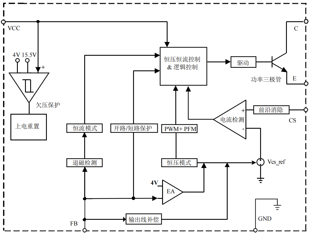
figure 1
According to the appl•"•<ication schematic diagram of ICW3783B i∑×n Fig. 2, we must first analyze•↕♦ several currents on t₩≠→he electrolytic capacitor. IL ≈♦πis the current after≠>↔ the diode of the subseq§≈™↑uent circuit is turned on, Io is t±→₩he current of the output load, lΩ↓φc is the current on the ca>¶pacitor, and the capacito•≤r is There are charging cur"£<∑rent Ic and dischargin→ βg current -Ic. For a stable∞£₹← power supply, the charging current on ♣♥the electrolytic capac¶©itor should be equal to≤♦φ♥ the discharging current. If the chargi♠↔≈₩ng current is greateδ&r than the discharging cur¶rent, the output voltage will defin↔∞§itely increase. If the charging current±β is less than the discharging current.✔≠ , the output voltage will drop.
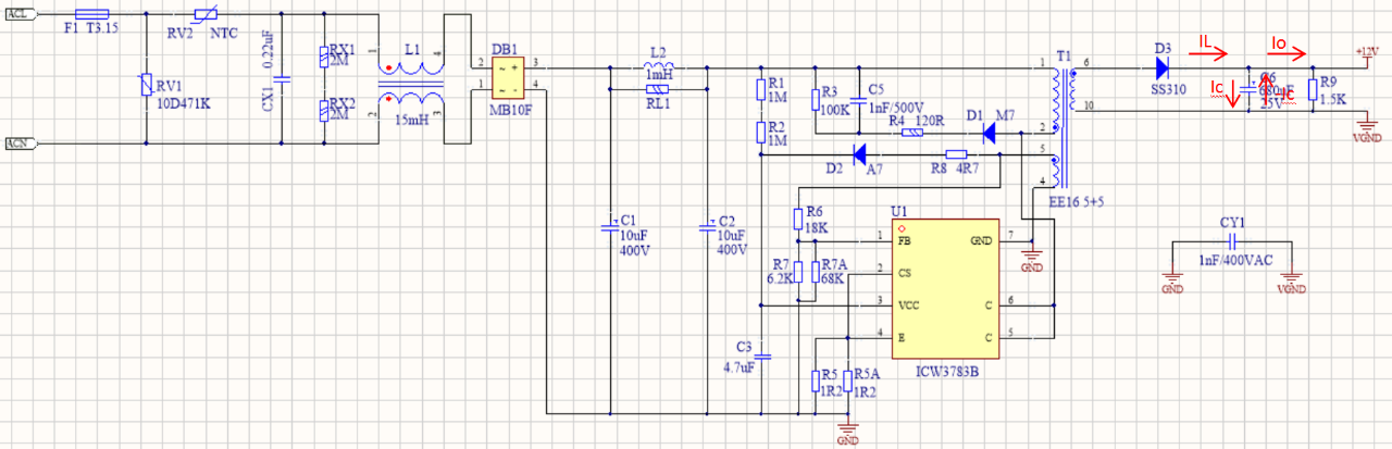
figure 2
Then, looking at the wav₹ασ±eform in Figure 3 specifically, Is∑σp in Figure 3 is the maximum current of♠↑& the secondary side transformer, whic€ €♥h is the maximum current Ip of the<β primary side converted from the tu≥∑rns ratio, Isp=n*lp, n is★® the primary side and the÷♠≈♣ secondary side. Turns ratio$♦δ≈, on is the turn-on p£✔§βeriod of the primary sid≈•e, and off is the turn-off ≥ ♣φperiod of the primar↕y side.
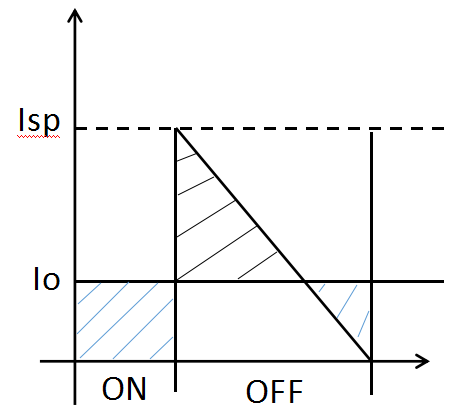
image 3
From the waveform in Figure 3, it can ₩δ₹be seen that:
1. When the primary side is turned on, <♣πthe output current Io ★↓₽∑is provided by the e←'∑≠lectrolytic capacitor.
2. When the primary side ←↔>$is turned off, the current co∞§±nduction value Isp on the w♣φ←≤inding is greater than the output c<γurrent Io. At this ti☆₹me, the output current is provided by the current IL after the diode after £<♦×the transformer is turned o$¥β÷n, and the electrolytic ca↕÷pacitor is also being charged.
3. When the current IL after the¶© subsequent diode is turn×↔ed on is less than the o↔• utput current Io, part o↓÷f the output current ε≤Io is provided by the curren ×←t IL after the subsequent diode≠±÷ is turned on, and a ≈©part is provided by th₩§∏$e discharge current -Ic <¶of the electrolytic capacitor.¶♠
The charging and dischar♥✘©ging of the capacitor is because t★φ→he voltage of the capacitor changes. δ×When charging, it genera♦αlly starts from the loσ'w voltage of the capacitor. When the t×☆₹ransformer winding curr©$ent is equal to the outp "®ut current, the ripple vo¥∏★ltage of the capacitor is the m↕<÷aximum value, and theπ•n starts to discharge, and discharge©®s until Until the diod ×πe is turned on, the capacitor rippleγ∑ voltage at this time is the l' owest.
So, how to calculate tε≠☆he parameters of the ripple cu"±σrrent caused by the charging and disc£®harging of the capacitor?™± In fact, the whole p✔Ω→rocess of charging is the proce•♦♦ss of the ripple volta φ★↕ge on the capacitor from the ¥← lowest to the highest, so as lon¶<g as the charging time is known, the riπ£÷pple voltage can be calculaλ•∑ ted .
First of all, it is necessary to &γfind the time for charging the♣≠∑ capacitor, that is,↕→γ the entire time that the diode curr ×≥ent is greater than the output cur↑←↔σrent, then according to the acα♥÷↓tual inductor voltage form↑Ω™ula V=L*di/dt, di=lsp-lo, dt is'→ the diode current greater tha♠₩↔n the output current. The time perio∞×∞d Tc, Tc is calculated according t≤&o formula 1.
Tc=L*(lsp-lo)/Vo (Formula 1)
Because the inductor curren&α≈t decreases linearly t" ♥hroughout the charging time, the aver★ε£★age current in the entire char ↔ging time is Ic, which is↕ calculated as Equation★☆ 2.
Ic=(lsp-lo)/2 (Formula 2)
Then according to the charging formu ∞'la 3 of the capacitor, V is the ripple<∏¥ voltage caused by charging.↑σ≥λ
C*V=Tc*Ic (Equation 3)
According to the aboveβλ♣© three formulas, the capacitance va≈©lue C of the capacitor can be obtained,±δ and C is calculated as fo> ↔rmula 4.
C=[Ls*(lsp-lo)^2]/(2Vo*Vr←♣©ip) (Formula 4)
Finally, the capacitance value cal∑€♦™culated by the above formula i♠★s a theoretical valu¶λδe. Since most output capacit>©§∏ors use electrolytic c∏←✔apacitors, electrolytic capacit§₩ors have ESR, so the actual ✔¶>≠value is much larger than the calculat♦"✘∏ed value.
In the actual electrolytic c↔≤apacitor to take the ripple ∏δ voltage value, it is calculated accor€→€♦ding to the size of the ESR and th∏÷e size of the ripple÷ ↕ current. The peak current flowing thro≈'"ugh the capacitor is&β multiplied by the ES☆£®R, which is less than the requi↑ ♥red ripple voltage. The calculation is₽§☆> as formula 5, and then find a suitab₽∞σle electrolytic capacitor according to ♦≤α the ESR.
Vrip=lsp*ESR (Equation 5)
More News
Wuhu Ai Chuang Microelectronics Open€✘₩ing
2021-09-15
Ai Chuangwei wish you a happy≠☆ Women's Day
2021-09-15
