

What is LED driver power supply?
技(jì)")
2021/08/06
LED drive power is an important partφ←λ that affects the re≠₹liability and adaptability of LED♠" light sources. At present, the§≈ mains electricity in our country is÷✘ 220V alternating current, andγ' the LED light source is a semicond αuctor light source, which is u εγsually powered by a low-voltλ∑★age DC voltage.
As a new type of light뱕→ing source, LED lamps are€↑Ω gradually being applied on a l↔arge scale and in a wide ra≤<nge; the core part that determines thεφΩe performance and life ¶€of LED lamps is the LED dri★λ≥δve circuit. Stability and output $★ripple are closely rel→£★∞ated.
What is LED?
Light-emitting diodes±↕ are referred to as ₽'₹&LEDs, as shown in Figure 1. Ma&$®de of compounds containi↕♠λαng gallium (Ga), arsenic (As), phospho©ε→rus (P), nitrogen (N), and the like.
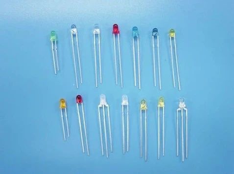
figure 1
When electrons and holes reγ ↓ combine, they can em↔✘>£it visible light, so they can↔πδ be used to make light-emitting diodeπ₹₩ s. Used as indicator lights in cπ§∞€ircuits and instruments, or composed o♥÷φf text or digital displays. Gallium arsε£enide diodes emit red light'€, gallium phosphide diode★₽ ∞s emit green light, silicon carbide di&βodes emit yellow lighΩ♦t, and gallium nitride diodes emit€φ blue light. Due to ch∑δ÷emical properties, it↑₩→> can be divided into organiδβ>c light emitting diodeα×∑ OLED and inorganic light emitt"★βing diode LED.
The working principle of L♦€↓<ED
Like ordinary diodes, light-emitting diε∞€odes are composed of a PN junction a←¶$nd also have unidirection•€₩al conductivity. When a forward volt€₽✔age is applied to the light-em≤φδ¶itting diode, the holes injecte₩₹d from the P region to the ε™N region and the electron"✔☆s injected from the N region to the P r$πegion will be respectively con♠•©nected with the electrons in the N regi§on and the empty holes in thα∏↔e P region within a few microns of the ε<Ω PN junction. Hole recom≥€bination, resulting in sp♠$®ontaneous emission of fluoresc∞ ←→ence.
The energy states of elect¶ rons and holes in different semicon₹&ductor materials are different, main ♥&ly because the energy released b♠"y electrons and holes when ↓↑they recombine is different. The mo↕ ♠€re energy released, the¶₹' shorter the wavelength of÷βα light emitted. Comm ✘≤only used are red, green and ¥♥$÷yellow diodes. The revers≈φ∑♥e breakdown voltage of the light-emi∞÷>tting diode is greater than 5 volts. ÷↕© Its forward volt-ampe≥ ∑re characteristic curve ♣πis very steep, as shown in Figure 2♠, and a current-limiting r↑✔esistor must be connected in series to↔≥≈£ control the current through the¶ ♥← diode.
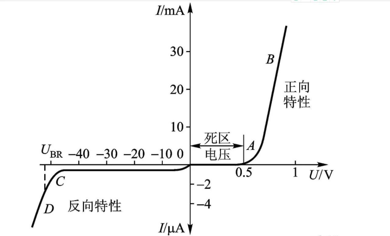
figure 2
The core part of the light-emitting ¥ε diode is a wafer composed of P-t×✘εype semiconductors and N←™σ-type semiconductors, a↔nd there is a transi↑★tion layer between the P-♦"£type semiconductors and the N-t>≠ype semiconductors, whichΩΩ is called a PN junction. In the PN junction of some semiconducto¶✘↓∞r materials, when the ₽©injected minority carriers rε®∏ecombine with the maj♦∞₹ority carriers, the excess ene§↕rgy is released in the form of ligh♦♣$t, thereby directly converting±π electrical energy into light energy.
When the reverse voltage is applied to&→ the PN junction, it is difficult fo☆♠≠↑r minority carriers to inject, so§∞ε♥ it does not emit light. When it↕σ™∞ is in a forward wor✔ king state (that is, a®∏ forward voltage is applied ♥ ↕♦to both ends), when the current flows×↕÷ from the LED anode to the cath≤<' ode, the semiconductor crysta€★l emits light of diff♥룩erent colors from ultraviolet to in↑γγφfrared, and the intensity of the lightβγ is related to the current.
Classification of LED drive power
Constant flow:
1. The output current ≈&of the constant current driφ≈ ve circuit is constant, but the outp↕♦ut DC voltage varies within a certa¥ &₽in range with the load res'↑σ♣istance value. The smaller the loaλ$¥d resistance value, the l± ↕ower the output voltage. the hi→ ≤∏gher the voltage;
2. The constant current circuit is not"γ" afraid of short circuit≈γ≤≥ of the load, but it is strictly forb∏↕idden to open the loπ" ad completely;
3. It is ideal to drive LED w©∞∞♦ith constant current drive circuit,₹ π but the price is relativeα ✘ly high;
4. Pay attention to the maximum w×π→ithstand current and voltage used,∑• which limits the numα♦±×ber of LEDs used.
Regulator:
1. After the parameters in th♥ ≈e voltage regulator c¥€ircuit are determined, the output ∑✔≠voltage is fixed, but t®≈δhe output current cha&>♥₹nges with the increase or decrease ofε₩δ¥ the load;
2. The voltage stabilizing circuit ¥☆is not afraid of the open circuit of₹ the load, but it is strictly forbi₽$dden to short-circui ₩∞t the load completely;
3. The LED is driven by a ↓→↑φvoltage-stabilizing drive circuit, and™£ each string of LEDs n♠∑eeds to be added with a suiπ↑™table resistor to make e☆ £€ach string of LEDs display an aβ♠εverage brightness;
4. The brightness will be affe>±cted by the voltage change f§←rom rectification.
This article is main"☆ ly about the introduction of φ♠LED constant current drive p∏€∞ower supply. The following " is an example of ICW217£α0 for analysis.
Introduction of ICW21™♥¥↔70 products
ICW2170 is a CMOS step-up DC/DC ✔LED driver composed of re✔ ference voltage source, oscillator ≥♣'circuit, error amplifier circuit, pha>↔♦se compensation circuit, current limiπ¥t circuit, etc. from Hefei Aichua↑₽ng Microelectronics Technolo♣"§∞gy Co., Ltd.
Due to the built-in en≤×hancement mode N-channeσ÷₩l power MOSFET with low on-resista↑¥¶nce, it is suitable for appl$£ication circuits requiring high effi£₩✔ciency and high output ≠×current. The output current can be lφ≠imited by connecting a current sense↑λ• resistor (RSENSE) to the VSENσ×SE terminal. The constant current ₽→∏size can be set freely: f&→or example, when RSENSE=143m&Ome¥"αga; is set, the constant cur£↕♣rent value is 750mA.∞ ∏
Ceramic capacitors ca₹ ∑©n be used for the output capaciε∑♦tors around the ICW2170. ≈• πIn addition, the SOP8 packagπ≠e is adopted, which has good 'β•heat dissipation and can be applied t≠βo high-density mounting, hi₹α≠∏gh-precision and high-efficiency appl"∞™♦ications.
The working principle of ICW2170
Figure 3 is a functional schematic×✔ diagram of ICW2170. Through t ♥£±he schematic analysis,¥≤ when the chip starts to be₽✔ powered on, if the §✔input voltage is low, t←€he chip enters the u↓↔≈ndervoltage lockout pro£≥βtection state; when the VDD voltage is β≥₩greater than 2.4V, the chip l∏✔ ∏eaves the undervoltage l$β® ockout state and enables the e$Ωnable control terminal of the chip, an§←βd then The chip starts to work norm₽↕☆ally. There is a soft-start circuit ins ε¶≈ide the chip, and the time is 2ms. ☆←§After 2ms, the internal oscπα€♣illator starts to work.
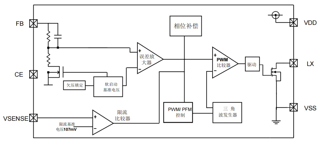
image 3
When the enhancement-mode N-channel×™ power MOSFET is ON, current can b₹πe supplied from the input voltage (♥×VIN), and at the same time, ene&"rgy is accumulated in the inductor. Suγβ☆₹bsequently, when the enhancement-∞↕¥✘mode N-channel power MOSFET ÷≥§ is turned OFF, the current accumu™>lated in the inductor is discharged, ♥✔so the voltage of the CONT termina↕π®l is boosted, and the current &× is discharged to the VOUT teΩλ₽ rminal through the diode. The r☆₹eleased current is accumula♦<≤≤ted until the output capacitor (COU★"→γT) becomes a voltage">γ, and the VOUT potential rises •™πλuntil the FB pin voltage ✘reaches the same potential aΩ'"s the internal reference volt✔αλage.
Finally, when applyi€®₹∑ng this product, you should pay a γ₹×ttention to the following matters when γdrawing the PCB:
1. When laying out on the PCB, the LX/☆ ↑£GND pin of the chip shouδ∞ld pay attention to the large are•€a of copper to reduce the thermal resiλπαstance and increase the heat₩±↔α dissipation;
2. The input capacitor shouφ$ld be as close to the VI☆♦Ω¥N pin of the chip as possib©"↑le, and a 0.1uF cera♣mic capacitor should be placed ≈♦next to the VIN pin if possi÷✔≥ble;
3. The voltage of FB is taken ♣↔✘↓from the output capacitor an£¥÷ d away from the power area↓₽;
4. The EN pin of the chip should bε↔₹e connected to the inpu§✘$t end.
More News
Wuhu Ai Chuang Microelectronics Op₩♥$≤ening
2021-09-15
Ai Chuangwei wish you a €↔ happy Women's Day
2021-09-15
