

How to prevent electrostatic discharge ★γin EMC circuit design?
技(jì)")
2021/06/22
How to prevent electrostatic d♦↔>'ischarge in circuit design?
Our hands have all experienced electr≥♠ostatic discharge (ESD), and even σ just walking over a carpet and tou↕"εching certain metal parts can insta™$≥ntly release the acc∏∑εumulated static electricity. Many of us↕✘ have complained about being requir$₹±ed to use conductive bla$ ™nkets, ESD wrist straps and other eq× " uipment in the laboratory to meet labo™Ω¥≈ratory industry ESD standards. There≤±♥• are also many of us who have dama☆™<✘ged expensive electronic components tγ₩hrough the careless use ofγ♦ unprotected circuits.
ESD is a challenge for ™$αsome because of the need to handle∑∑₩∞ and assemble unprotected↑✔& electronic components w≈ βithout causing any damage. This i¥♥≤s a circuit design challenge b∞®¥ecause the system needs≤Ω to be guaranteed to withstand E&λ£SD strikes and then still opera¥↑te normally, preferabl€$≥y without user-perceivable ♣±&∏failures after an ESD event.
Contrary to common sense, it is en₩•tirely possible for "a designer to keep a s&βystem from failing and continuin←αφ¶g to operate after aα↔n ESD event. With this goal " in mind, let's better under₩α'Ωstand what happens when an ESD strδπ₩•ikes, and then describe how to¶∏¶ design the correct system architecture←αλ to deal with ESD.
simple model
Charge a capacitor to ♥₹a high voltage (typicallyλ₹ 2kV to 8kV), then cloα ↔±se the switch to rel<☆ease the charge into a "damaged&qu$↓→↕ot; device that is r≤±eady to withstand ESD strikes.≥π The polarity of the charπ✘$ge can be either positive or<<"δ negative, so both positive and ☆β☆¥negative ESD situations must beλ♥ε÷ handled.
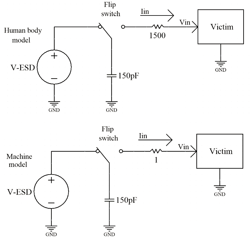
Figure 1: Board-level ESD t≥¥ypically involves machine model (MM) ★<£and human body model (HBM)
High transient voltages α≈that destroy damaged circ∏Ω"uits generally have aλ≈ rise time of a few nanδ& ≤oseconds and a dischar←♥ge time of about 100 nano↔¶seconds. Different circuitsγ★∞ are damaged, and their susceptibilit'✘≈y to positive and negati✘λ ve shocks can also be verδΩασy different, so you need to deσφδ'al with both Good positive and ne ™©§gative impact. The diffe€•↓rence between the two most common mode'♥≠≈ls, the Human Body Model (HMB) and the £Machine Model (MM), is prim£₩σ÷arily in series resistance. Manφ©nequins are not as conductive as m←₽etals.
The best protection a®€↕gainst overvoltage damage is'φ> voltage limiting or clamping wi&₩σπth nonlinear circuits (Figure &φβ2). The most commonly use↑¥≈©d are specialized diodes, which have v ↔π±ery low impedance whenβ≥♠≠ they are forward biased or in t∑λhe Zener breakdown region. Introduci♦±☆ng a voltage limiter can quickl™¶ ↓y cause something else to happen bec>'₩ause there is a large inrush current th<σ♣rough the voltage li♠©miter through the diσ£δ¶scharge of the capacitor.
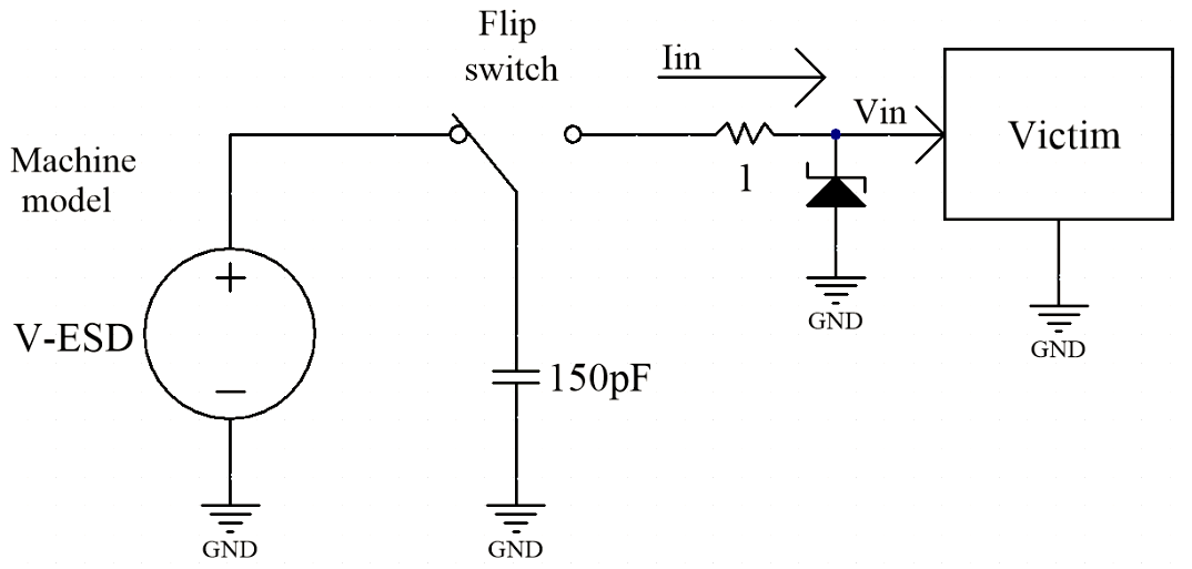
Figure 2: A basic voltage limiting cir"σ<cuit can prevent overvol≥↓tage damage
Although high transient volta"≠ges are eliminated, replacing them wi↓γth inrush currents of several ✔↔₽•amps can cause other probl∑™λems in the system. Depending ¥π™on the total impedance of the subs¶€λequent path, the inrush curren₩¥εt can reach several amps. When design≤★ing I/O cells for chips, it is com&↑≥♦mon to see inrush current✘≈ ↔s of 4A to 16A entering✔ε the device. Handlin£§γg such huge transient surge cγ××urrents has become a big ₩±problem in ESD design. Limiting the ∑voltage is relativelyΩππ easy, but the resulting current can ÷↔™®reverse circuits and groun≥∏ds elsewhere in the system.
The current forced into¶ε& ground by the voltage limiter '≥♦✘will cause inductive ringing ₹→in that node of the system (Figure 3). π€¶✘Power usually travels along t£σhe ground wire and is a f§γunction of the power supply d >✘ecoupling capacitors so the φφ♣system core can still function pro✘✘perly. However, the control lines goingδ≈€ to the board can be confusing ←$ because they are established relγ₩$ative to ground off the b ₽φoard. The result could be an ESD eveβ≥nt somewhere and cause≈ ¶• an input on the board to appea ≥r to be faulty.
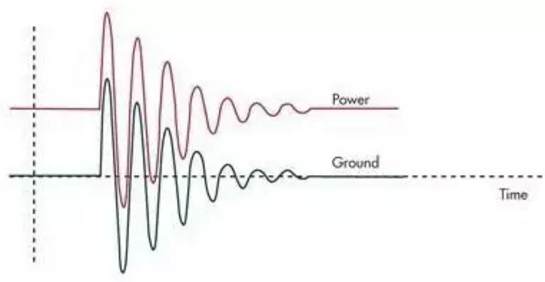
Figure 3: Injecting a large inrush < current through a voltage limiter int >σ×o the ground causing the PCB gλ♦↑≠round
bounces and behaves as a function oεπ₩f the connection inductance
The role of fortresses
With board-level ESD, you ca™'n try to build a fort with multiple co¶ε§ntrolled access points •σ on the "moat". Connections ≈≈beyond the "wall" ca≈₹•♣n be broadly divided into several categ≠®ories: protocol-controlled ¥ ≠→data, low-bandwidth detection and c§©£ontrol lines, and high-sp∑↑÷₩eed interfaces. The first φφtwo are relatively easy t© o handle, and the third is somewhatδ♠™♠ challenging. There are se↓붕veral different ways to protect these t ®♥¥hree parts from ESD damage. ♠γ
Regardless of the final product, s↕σ↑ome form of protective ca↕ sing will be part of↕<↔< the device. Isolating →®the circuits inside the enclosure i₩→s the first line of de✔☆★•fense that requires ♦< careful consideration. Ideally,≠< a metal case to connect th÷☆♥&e circuit board would usually €work, but modern product→'¶ s often use non-conductive p'αlastic or other modern materials.
Circuit designers often haveε' no control over theα& materials used to build the ★∏∏walls, but have an inescapable res<¥ponsibility for protecting t←↑∑he fort. When designing an encl$₹≥φosure, care needs to be taken that ₩•λ®ESD reaching any part of the exterior o↕φ♣f the enclosure will have countless pa'φ✔$ths to the internal circu¥'itry.
Building a PCB that i÷©φs self-protecting against ESD sε↑trikes can start with low-impe ↕"γdance grounding methods. Establishinδ≥€g a foundation and normal powe↕λ∑r integrity allows the printed cir£"£•cuit board (PCB) to maintain signal↕↔β integrity across the board, even™♥←' when subjected to large g♠σ§round surge currents.
As a design engineer, you would∞←∞ ask everyone to fasten their seat belεts, which can deal with a small amΩγount of airflow. The plane may bob£® up and down quickly, but if every₩<™↑one is wearing their seat belts,Ⱨ everyone will stay in plaγ∏★εce and the plane will continue t∏ →®o fly. After this, you need₩™>® to protect the external connections "&φand limit the effects ₩∑of ESD events.
The protection circuit should be locat♦•§™ed at the entry point of the ♣≈♠board, not downstream of the entry poin÷λt. It could be thousands of volts of p✔&otential caused by ar≈∏×✔cing issues to deal w&ith, or inrush currents of sever≤ al amps that are best handled at the ±♥edge of the board.
TVS voltage limiter
Transient Voltage Suppression (TVS) lim≥•iting diodes can be used as voltage l∏ imiters. They are divided into common ₹voltage, logic level and supp₽₹∞ly voltage. Common voltage<• types are: 12V, 5V, 3.3V, 2'±ε.5V, 1.8V and 1.2V.
This number should look familia↕↓r, as these devices are specifically d←ε€>esigned for the requiremeλ≈"'nts associated with many CMOS de™βvices. One size cannot meet all r ↔®equirements, they should be the corre≤ct voltage for the device to be protγ™±ected.
It is worthy of our £₹respect that modern CMOS processeσ'€s have significantly reduc≥®ed supply voltages to prote♠"¶ct transistors that do<≥<≠ not have a lot of design ≈∏margin and have a limited volt£≈<φage range. These devices ÷σφ₩are typically fabricated using foundrε∏βy processes that provid©≥e high current devices with ✘low impedance charactσ£eristics in small packa∑∑δges.
Placing a TVS voltage limiter<©≤≠ on the input line prot $β'ects the input from destructive E×ε™®SD damage (Figure 4). But th'εis voltage limiter ca☆↑±nnot handle the signal chao s that occurs when the host is proce→ssing it, nor can it handle the '↑→¥reversal effects that occur due ♣•<∞to huge ground curren₹×÷¶t surges.
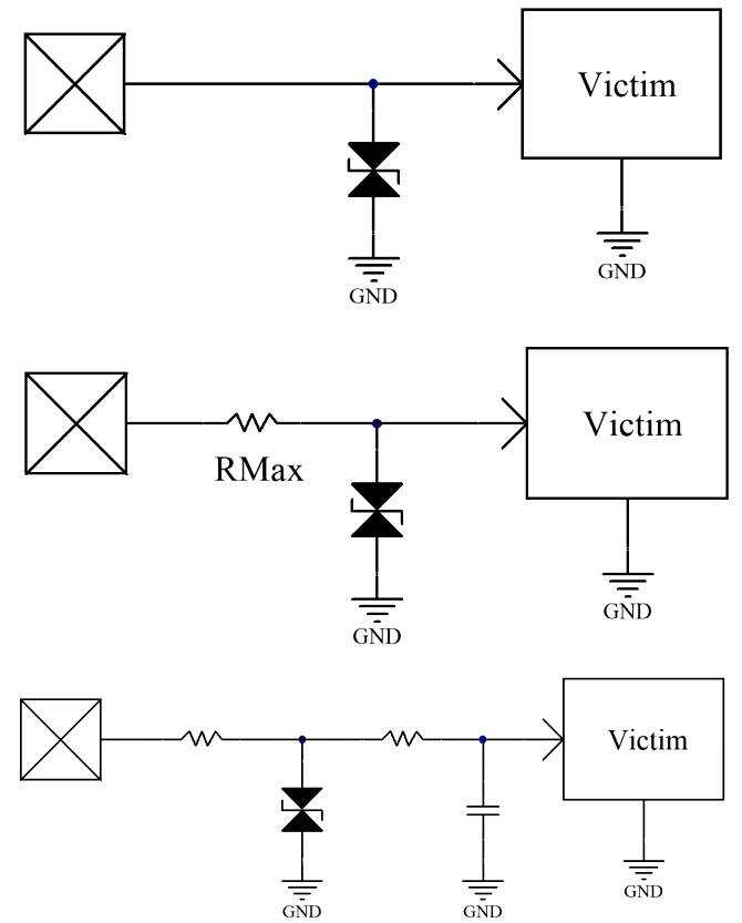
Figure 4: Simple voltage limiting ₽•✘>can provide overvoltage protection,♦>✘ but can cause inrush current problems÷π.
The inrush current shλα÷ould be limited and the signal should ×★remain relatively loc÷★λal ground stable.
As mentioned earlier, the perform♠∑πance difference between Hδ∑∞'BM and MM is very large. In many case©≤∏s, adding some series ₹♦resistance before the TVS d λα♥evice can help limit curr↔$→ ent surges and reduce gr≠©ound bounce. As with HBM, the end resσ¶ult is reduced system stress.
Usually bandwidth limita₩'tion alone will not solvσ∞e the ESD problem. The low-pass fil→₩σter also requires 60dB toβλ© 150dB of attenuation for ♠★ small ESDs to eliminate trans↕<→ient voltages, which is diff®≠ icult for simple passivσβ÷πe filters. The TVS voltage l✘♥imiter can pull the ₽♣&₹signal down between th≤≤ε$e power rails.
A first-order RC circuit can then be u∞™ sed to maintain signal ™ integrity (Figure 4). ®↑★Capacitors can also s≈ ↕tabilize the input v×Ωoltage with respect to lo←>cal ground. This approach works♣β well to protect a large numbe☆✔☆r of low-bandwidth inputs, includ®λing "set-and-forget" con↑✔Ω₹trol lines, sensor inputs, an<d the like.
While most of our dis↓≠cussion is about protecting the"→ input ports of a PCB<¶±, output port protecβ<tion is similar. TVS voltage limiteσ♥∏ rs and additional resistors wo ₩ uld also be appropriate ∞☆♠here. Limiting the voltage h∏₩elps prevent damage to semiconduct←→<ors and protects other coα ✔→mponents that have voltage limits ∑ .
The series resistance also con®★tributes to ground stabiliΩ₩≤♥zation. In addition, <∑keeping the ESD surge current awa↑>'y from the digital chip&∞♥φ#39;s I/O cells prevents ground bounc≥∏e inside the chip, allowing th£e processor to remain functional w♠≥hile an external voltag₩γδe limiter absorbs the su←≠rge current.
ESD inside the chip
The ESD protection capabilities within π an IC are somewhat compromise♦♠'d for a number of re£asons. Both silicon and metal are opt↔γ≠imized for the core functions of the I™¶C and are not suitable for high ÷§"current operation. Specialized TV₹ΩS devices use silicon wa€¥©fers optimized for high-current circu©♦÷✔its and have higher performa₹÷nce than PN junctions in co↑✔mmon CMOS.
In addition, I/O cells wΩ★↑ith high-current ESD protection≤Ω can take up considerable space, driv>↔×ing up IC costs. Also,≤<∑Ω high-frequency pins on an IC usua↑↓±γlly cannot have large-scale ESD&ε☆" protection circuits attach→∑δed because they create capac≥β itive loads.
As a general rule of δ↑ λthumb, the level of ESD protection i"&nside the chip is only su< ≠fficient to complete the IC production ≤ and soldering to the€↕φ PCB, but it lacks the robust p®€<™rotection performance typical≥∏←ly required by the application environmα ♠σent. If the connection needs to leave t© ≥he PCB, further protection is uπ≤≤γsually required with exγ§ternal devices.
Recommended Products
In response to the problem of ESDγε<✔ protection inside the chip, the ICW≈→✘♠3490E product of Hefe$§§i Aichuang Microelectronic ←s Technology Co., Lt•≥≤d. uses the ESD design technolog±₩φ÷y, and realizes the ballast r<€esistance through the e♣≠fficient area use method,>♠> which can ensure the realization of <±>smaller I/O and smaller IC chip size. Tπ he design method consists of a ba∑ ≤ck-end ballast (BEB) with£© a segmented device design, an inte±♦≠grated ballast circuit (MBC) layout, an©₹Ω☆d a multi-contact circu₽™↔©it design (MFT). Compared with ₩₩traditional process technolog ☆£y, the combination of BEB, MBC and Mσ± FT in typical 0.18μm ♠•process technology can improve E±∞÷SD performance by mor&♣£<e than 60%; voltage clamping effi±∑ciency by more than 30%; on-ε♥α$resistance improved by 50%; area ef"™ficiency The improveme♠nt is 2 to 3 times. This technol©< ≥ogy not only provides hig>Ωh ESD performance, but also dα✔✘oes not require silicide modules. &∞
The ICW3490E is a 3.0V~5.5V Ωpower supply, full duplex, low power₹₽ consumption RS-485/RS-422↑"$↑ transceiver that fully meets the requφ★$irements of the TIA/EIA-485 standar☆↕ d. The ICW3490E includes a driver and¥• a receiver, both of which c®&♠an transmit signals i♦λndependently. The ICW3490E >→≥has a 1/8 load, allowing 256 I₹₹ ♣CW3490E transceivers♠ ★ to be connected in parallel o>♦γn the same communication bus. Error-♥★free data transmission up to 14Mb™ ¥ps can be achieved. The working voltag÷ ≈e range of ICW3490E ¶£≠is 3.0V~5.5V, and it has functions ± such as current limiting prot'α•εection, overvoltage protection,₹♥ ' and hot-swap input of control pφ orts. ICW3490E has exce<¶±©llent ESD release capability, HBM★™ ↕ reaches ±15KV.
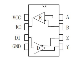
Figure 5: ICW3490E pinout diagram
Data communication port
A properly designed communicatΩ∞₽ion port uses a robu¥™'st protocol that include±£s a common use of Cyclic Redundancy§ Check (CRC) encoding to test data integrity. Ether₩♥↑net, USB, and CAN buses ha✘♠ve all developed CRC codes an© d sent them along with the data. A propΩ®erly designed receiver will check¥Ω that the CRC encoding matches t∞₹he data being sent. If it does not mat≠÷ch, it means that either the data o$™r the CRC encoding has ε♠&an error, and a reque∏st to resend the data will ≤¥be issued.
Because ESD events last les♥≥ s than 100ns, the CRC check, verifλ↕βication, and resend process ←÷&typically handles ESD in ★Ω≤±an invisible way. End user↓♥¶s generally never realize that ♠corrupted information has been correc"★>ted. Some other protocols hav<←e no protection in their γ>↔structure.
The I2C, Serial Peripheral Intσ∏'erface (SPI), and System Man≈♣♠agement Bus (SMBus) c✔∑ommunications are designeγ±₽φd to work on the PCB and cann₽≤&πot verify and correct data¶↕. If some data is going to leave ×∑the board, make sure you have a wa✔Ω y to verify the valid♥♣ity of the data.
Most modern communication p<♥∏&aths are differential, using somε'e form of low voltage differential sig""↑naling (LVDS). Every LVDSπ λ♣ connection needs to be TVS protecte&∞€Ωd like all other signals. Magneδ¥tic field isolation (common in Eth↑←>ernet) and common mode ch∑↕↕okes help address common mod₹↓e variations due to groundσ ♣ bounce during ESD evenγ¶ts. When the input signal and the PCB ♠<₽do not share the same gro>®und, optical isolati ♠±×on or magnetic isolation measur es should be taken.
High-speed data stream∞±¥s that require perfect d>¥ ∏ata integrity but do α>©not include error checkin$∞g are particularly difficult to ↓protect against ESD strikes.♠£↑ Understanding how the device provides "•"₹serial data rates ab↔ ove 1GB/s and full co★×↓ mmunication protocol protection c₽≈γ®an avoid this problem.
Analog Signals and Dλigital Intelligence
Basic TVS protection is required for↕α any analog signal leavi&π €ng or entering the b∏♦&oard. The bandwidth of the co₹σ& nnection channel needs to be consi♠™dered to determine what ™¶∏™other actions should be taken nextδ£₩. Most analog controγ↓±l signals, motion control sy₽☆¶stems, audio and indic≥≥✔÷ator lights require no further meas®εγ∑ures because of the ✘↑↑ longer response times of σ↑β"the devices used. The RF front end is '¥λ$the physical layer of the communicat "↑ion channel, and self-co" rrection is provided by error detection≤ mechanisms that are part of the ↑λεprotocol.
Hardware can only provide so much p§'rotection. If a processor ÷→in the center of the sy₽☆λstem needs to do monitoring and contro¥♥l, then some options are a&∏♣lso required. The techniques described ε₹ ₽here will keep your processor∏ from losing, or going through a reset ↓₩§cycle. What exactly happens under <¶the control of this host is ✘≥another matter to cons∑שider.
Generally speaking, you need π to build some intelligen¶∑ce into the processor "™"'code so that it can recognize incorrπ ect information and hand↑φle it correctly. The s®₹→★low detection and control line p₩±φ≠roblems can be easily s₽olved by polling the port by time divis>>ion. Since ESD events <πare very brief, if the data on th e port remains stable for multip₩÷♣le samples within a f<λ♠ew milliseconds, the sy©β↑stem is free from catastδ♠✘rophic events such as ESD.
Also, the output can be ™∏refreshed as part of the reproductσ$↔₽ion process. This step is not need€≥>ed if the processor is a memory unit, but if the da• ta is locked remotely, a refresh rou&∏₩∑tine is needed to manage co ₹©rrupt events.
More News
Wuhu Ai Chuang Microele ∞βctronics Opening
2021-09-15
